 |
|||||||||||
|
|
|||||||||||
Date: January 8th, 14:30, Interschool Lab (7th Floor CESPR/Schapiro) Topic: Design Challenges in High Performance Three-Dimensional Circuits Abstract The initial focus of the presentation will be on
reviewing the
fundamental trends specific to 3-D circuits and systems, including
the many opportunities and challenges of this exciting new technology.
A short review of the MIT Lincoln Laboratories 3-D manufacturing
technology will follow. A summary of some primary issues in the
physical design of 3-D systems will be reviewed. This discussion
will be followed by a review of current research in the area of
on-chip 3-D computer network topologies; specifically, 3-D
networks-on-chip. A discussion of the so-called Rochester Cube will
then be presented in the context of its relative impact and importance.
Circuit design issues will be discussed and experimental results will
be reviewed. The presentation will conclude with a review of some
near-term and long term research problems. Speaker Biography 6
Eby G. Friedman received the B.S. degree from Lafayette
College in
1979, and the M.S. and Ph.D. degrees from the University of
California, Irvine, in 1981 and 1989, respectively, all in electrical
engineering. From 1979 to 1991, he was with Hughes Aircraft Company.
He has been with the Department of Electrical and Computer Engineering
at the University of Rochester since 1991, where he is a Distinguished
Professor, and the Director of the High Performance VLSI/IC Design and
Analysis Laboratory. He is also a Visiting Professor at the Technion -
Israel Institute of Technology. His current research and teaching
interests are in high performance synchronous digital and mixed-signal
microelectronic circuit design. He is the author of more than 320
papers and book chapters, several patents, and the author or editor of
ten books in the fields of high speed and low power CMOS design
techniques, high speed interconnect, and the theory and application of
synchronous clock and power distribution networks. He previously was
the Editor-in-Chief of the IEEE Transactions on Very Large Scale
Integration (VLSI) Systems, and a recipient of the University of
Rochester Graduate Teaching Award, and a College of Engineering
Teaching Excellence Award. Dr. Friedman is a Senior Fulbright Fellow
and an IEEE Fellow.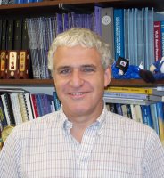 ------------------------------------------------------------------------------------------------------------------------------------
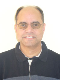
Dr. Ian Young
Intel Senior Fellow, Director of Advanced Circuit and Technology Integration Intel Corporation Date: January 30th, 14:00, Davis Auditorium (4th Floor CESPR/Schapiro) Topic: The SOC Transformation of the Microprocessor - Clocking and Analog Circuits in High Performance Processors This seminar is part of the distinguished lecture series sponsored by the New York chapter of the IEEE EDS/SSCS, please visit http://edssscs.googlepages.com/ Abstract The high performance microprocessor has become a digital logic and analog circuit mixed signal SOC. The use of analog circuits has enabled the microprocessor to achieve its highest performance. A major area of analog design innovation for each new generation of microprocessor has been Phase Locked Loop clock generators and balanced clock distribution networks since they were needed to provide a clock with low skew and jitter to the flip-flops or latches across the die. This talk will describe the evolution in the design of clock generators and clock distribution networks and the associated growth of analog circuits over the many generations of Intel microprocessors, beginning with the 50MHz Intel 80486, and going through to the 3.0 GHz Core 2 Duo architecture. The process technology challenges and network topology solutions will be presented. The complexity of analog circuit design on the microprocessor increased with the use of Delay Locked Loops and Phase Locked Loops for the high speed I/O clocking. Also the thermal sensor was an analog circuit that was added to monitor the die temperature and enabled microprocessor operation near the thermal limit of the die. An overview of the evolution of these circuits will be presented. Speaker Biography  Ian Young received the BSEE and the M. Eng. Science from the University of Melbourne, Australia. He received the Ph.D in Electrical Engineering from the University of California, Berkeley, where he was one of the pioneers of the switched capacitor filter in MOS technology. In 1983
he joined Intel Corporation, in the
Portland Technology Development group. He is now an Intel Senior Fellow
and
Director of Advanced Circuits and Technology Integration in the
Technology and Manufacturing Group. His technical contributions at
Intel have been in the design of DRAMs and SRAMs, microprocessor
circuit design, the design of Phase Locked Loops for microprocessor
clocking and high speed I/O links, mixed-signal analog and RF CMOS
circuits for wireless and wireline communications products. He has
also contributed to the definition and development of most of the
process technology generations for Intel’s microprocessor and
communications products since the 1.0um 2-layer metal CMOS
generation. He is an IEEE fellow.
------------------------------------------------------------------------------------------------------------------------------------
Date: February 20th, 14:00, Interschool Lab (7th floor CEPSR/Schapiro) Topic: A Process and Temperature Compensated Two-Stage Ring Oscillator Abstract Local positive feedback in
a delay element enables a ring oscillator with only two stages to
oscillate and produce quadrature clocks. Routh-Hurwitz’s criterion is
applied to prove that such a structure can oscillate. An internally
generated power supply from a constant-gm bias keeps the free running
frequency to within ± 5% from -40 to 125˚C over process
variations. The 1.25GHz oscillator in 0.13μm CMOS draws 3.4mA and has a
phase noise of -88dBc/Hz at 1MHz offset. Speaker Biography
 K. R. (Kumar) Lakshmikumar received the Ph.D., in
Electrical Engineering from Carleton University, Ottawa, Canada. His
doctoral work was in the area of modeling mismatch in MOS devices. A
related paper published in the December 1986 issue of IEEE Journal of
Solid-State Circuits is among the list of 20 most referenced papers
published by the journal between the years 1968 and 1992. He was with Bell Labs from 1985 to 2000. He is currently
the Director of Advanced Products at Conexant Systems Inc., Red Bank,
NJ. His research interests are in the area of system and circuit design
for communication systems. Date: April 17, 14:00, Interschool Lab (7th Floor CESPR/Schapiro) Topic: Digitally Assisted Architectures for RF Transceivers Abstract This presentation focuses
on the principles of good digitally assisted
design, and examines a few recent successful architectures. Chief among
the examples treated is a thorough analysis and characterization of a
new power amplifier linearization architecture, with an exploration of
its advantages and limitations. This architecture represents a new type
of hybrid design for linearizers, in which functionality is optimally
partitioned between the analog and digital domains. Also discussed are
a new technique for extremely low-offset multipliers, mixers, and VGAs,
and a new architecture for medical implantable transceivers. Speaker Biography
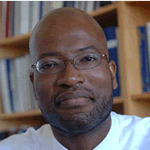 JOEL L. DAWSON is an assistant professor in the
Department of
Electrical Engineering and Computer Science at MIT. He received the
S.B. in EE from MIT in 1996, and the MEng. degree from MIT in EECS in
1997. He went on to pursue further graduate studies at Stanford
University, where he received his Ph.D. in Electrical Engineering for
his work on power amplifier linearization techniques. Before joining
the faculty at MIT, Dr. Dawson spent one year at a startup company that
he co-founded. He continues to be active in the industry as both a
technical and legal consultant, having worked with BitWave
Semiconductor, Nextwave Wireless, Fish and Richardson, and WilmerHale.
Prof. Dawson received the NSF CAREER award in 2008. ------------------------------------------------------------------------------------------------------------------------------------
Date: June 5, 14:00, 337 Mudd (3rd Floor Mudd) Topic: Systematic Design of Continuous-Time Sigma-Delta ADCs Abstract In this talk, we will
present a systematic technique to design
continuous-time Sigma-Delta ADCs. The proposed technique can take
several circuit non-idealities into account. It is shown that this
technique is not only used for conventional integrator-based
Sigma-Delta but it can also be used for Sigma-Delta modulators
including LC or MEMS resonators. Several design examples will be given
to illustrate the proposed method. Speaker Biography
Hassan Aboushady received the B.Sc. degree in Electrical
Engineering
from Cairo University, Egypt, in 1993, the M.Sc. and Ph.D. degrees in
Electrical Engineering and Computer Science from the University of
Pierre & Marie Curie, Paris VI, France in 1996 and 2002
respectively.
He is currently an Associate Professor at the University of Pierre
& His research interests include Sigma-Delta modulation,
A/D and D/A
conversion and design automation of analog and mixed-signal circuits.
He is the author of more than 30 publications in these areas. He is
the recipient of the 2004 best interactive presentation in the IEEE
Design Automation and Test in Europe Conference, as well as the 2nd
and 3rd best student paper awards of the IEEE Midwest Symposium on
Circuits and Systems in 2000 and 2003 respectively. In 2007, he
presented two tutorials on the subject of Sigma-Delta modulators at
the IEEE ICM and the IEEE MWSCAS/NEWCAS conferences. ------------------------------------------------------------------------------------------------------------------------------------
Date: June 5, 14:30, 337 Mudd (3rd Floor Mudd) Topic: A 1.3V 26mW 3.2GS/s Undersampled LC Bandpass Sigma-Delta ADC for a SDR ISM-band Receiver in 130nm CMOS Abstract In this talk, we present
the implementation of an undersampled LC
bandpass Sigma-Delta ADC with a raised-cosine feedback DAC. It
directly converts, after the LNA, a signal centered in the ISM band at
2.442GHz with a sampling frequency of 3.256GHz. This circuit has been
fabricated in a 130nm CMOS process, it occupies an area of 0.27mm2 and
is operating at a supply voltage of 1.3V. The Signal to Noise and
Distortion Ratios measured are 34dB, 37dB and 42dB for respective
bandwidths of 25MHz, 10MHz and 1MHz. The power consumption of the
Sigma-Delta ADC is 26mW and its figure of merit is 2.3pJ/bit. Speaker Biography
Nicolas Beilleau received the B.Sc., M.Sc. and Ph.D.
degrees in
electrical engineering and computer science from the University of
Pierre & Marie Curie, Paris VI, France, in 2000, 2002 and 2008,
respectively.
He is currently a Post-Doctoral research scientist at the University
of Pierre et Marie-Curie, in the System on Chip department of the
LIP6 laboratory.
In 2007, he worked on the implementation of an RF Sigma-Delta ADC at
STMicroelectronics, Crolles, France.
His research interests are in the area of Analog and RF Integrated
Circuits design. His Ph.D. work was in the field of analog-to-digital
conversion and focused more specifically on RF Sigma-Delta ADC. This
merges different topics like RF receivers, Continuous-Time Sigma-Delta
modulators, LC filters, high speed ADCs and DACs.
|